


4.5-V to 100-V Wide Input Voltage Range, 300-mA Current Capability! 3PEAK Releases the TPP0003X Series of High-Voltage Buck Products
3PEAK (stock code: 688536), a semiconductor company specializing in high-performance analog chips and embedded processors, has introduced its new high-voltage buck products, the TPP0003x series.
With support for a wide input voltage range of 4.5-V to 100-V, two optional operating modes, light load PSM (TPP00032), and FPWM (TPP00031), integrated overcurrent/overvoltage/overtemperature protection, and other product performance strengths, the TPP0003x series can be widely used in terminal scenarios such as PLCs, smart home appliances, servo drives, and can particularly meet the output requirements of the bus power supply systems of new-generation data centers. The 48-VDC output of the server power supply is directly converted by TPP0003x to generate a low-voltage power rail, reducing overall system complexity.
In the power supply systems of new-generation data centers, 48-VDC server power supplies are gradually replacing traditional 12-VDC supplies to reduce copper losses and voltage drops on the bus, and improve efficiency. Theoretically, under the same output power, with a 4x increase in output voltage, the output current decreases by 4x, reducing bus losses by 16x, thereby achieving higher efficiency and supporting higher power levels. However, the 4x increase in input voltage makes the design for the subsequent stage circuit very challenging. Designing high step-down ratios while maintaining high efficiency and high power density is difficult. 3PEAK's TPP0003x high input voltage buck converter series can meet the demand for input voltages up to 100 V and can support buck applications for converting 48 VDC to low voltage in data centers. Additionally, this series can be widely used in PLCs, smart home appliances, servo drives, and other scenarios.
Highlights of TPP0003x
Input Voltage Range: 4.5 V to 100 V
Continuous Output Current: 300 mA
0.7-Ω Integrated High Voltage Side and 0.3-Ω Low Voltage Side MOSFETs
Integrated 2-ms Soft Start
Adaptive Constant On-Time (COT) Control
Adjustable Output Voltage (Based on 1.2 V as the Reference Voltage)
Two Optional Operating Modes: Light Load PSM (TPP00032) and FPWM (TPP00031)
Integrated Overcurrent, Overvoltage, and Overtemperature Protection Functions
Operating Junction Temperature Range: −40°C to +125°C
Package: ESOP8
Typical Application of TPP0003x
The TPP0003x buck synchronous switch converter features all the functions required for low-cost, high-efficiency buck regulators, including integrated internal soft start, compensation, and protection functions. The typical topology is shown below. The converter is based on an adaptive COT control architecture. It provides fast transient response to achieve 300-mA continuous output current within a wide input power range, and exhibits excellent load and input voltage regulation capabilities.
TPP0003x Buck Topology
TPP0003x Efficiency Test
In industrial applications where the overall power consumption of the circuit design is crucial, TPP00032 demonstrates exceptional efficiency. Operating under conditions from 24-V to 12-V with an output range of 100-mA to 300-mA, it consistently achieves efficiencies above 85%, peaking at 94%. This meets customer demands for high efficiency. TPP00031 has lower efficiency than TPP00032 in light load mode, but is similar to TPP00032 in heavy load mode.
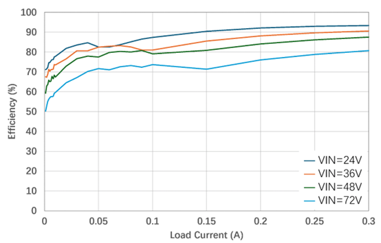
TPP00032 Efficiency Test
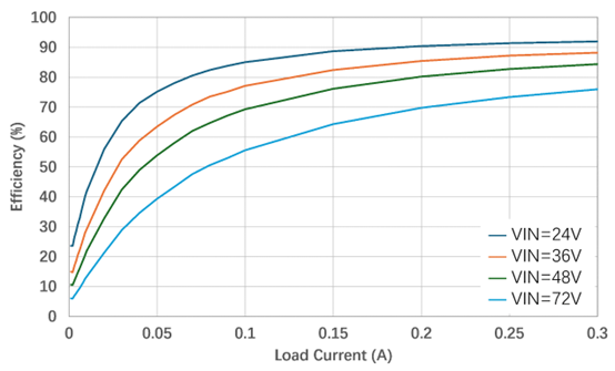
TPP00031 Efficiency Test
High Input Voltage Range and Low Load Regulation Rate
TPP0003x adopts an adaptive COT control scheme to provide excellent transient response and achieve ultra-high step-down ratio. Meanwhile, the output voltage changes minimally with the load current, meeting the requirements of various applications under different loads.
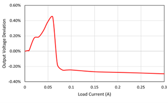
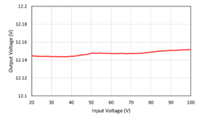
TPP00032 Load Regulation Rate, VIN = 72 V, VOUT = 12 V
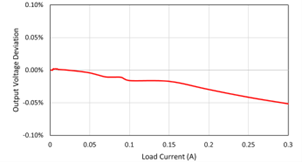
TPP00031 Load Regulation Rate, VIN = 72 V, VOUT = 12 V
TPP00032 Input Voltage Regulation Rate, IOUT = 100 mA
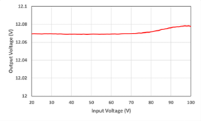
TPP00031 Input Voltage Regulation Rate, IOUT = 100 mA
PCB Layout
Key points of the TPP00032 PCB layout:
Connect the input capacitor across the VIN and GND pins with the shortest distance to achieve a minimal input loop path, reduce the interference caused by the pulse current of the input loop, and improve the overall stability of the solution.
Place the divider resistor network from VOUT to FB as close to the FB pin as possible to avoid interference from long FB traces. The GND of the lower voltage divider resistor should be single-point connected with the GND pin of the device as much as possible to avoid the GND of the lower voltage divider resistor participating in the GND current path of the input loop, improving the overall stability of the solution.
Keep the SW wiring as short as possible, as it is a source of strong pulse electric field interference. Also, SW should be routed away from FB, EN, and other pins to improve the overall stability of the solution.
The boot capacitor should be connected as short as possible across the BOOT and SW pins, as it is the high-side power supply. Therefore, the shortest path helps to reduce interference and improve the overall stability of the solution.
Choose smaller specifications for the feedback voltage divider resistors, such as 1 K to 2 K, to enhance the anti-interference capability.
The TPP00032 EVM layout is as follows:
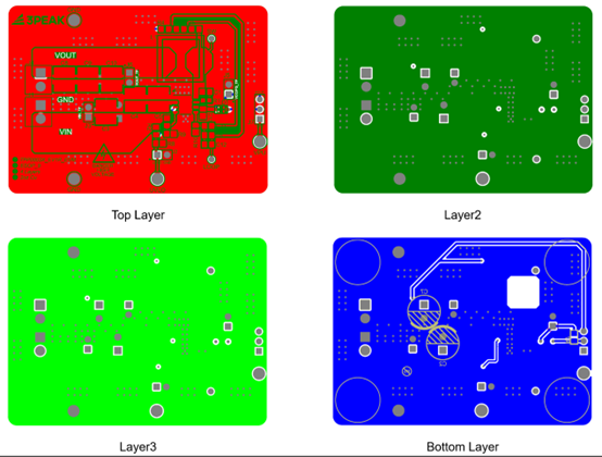
TPP0003X EVM Layout
The TPP00032 EVM board is shown below:
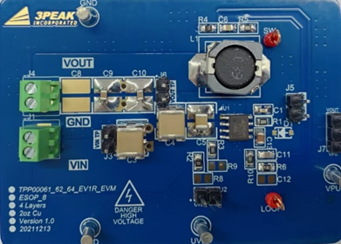
TPP0003X EVM
The TPP0003x is now in mass production. Samples and evaluation boards are available.


